Post by Yogi B on Sept 23, 2022 21:25:06 GMT -5
This is first of a few threads, in which the aim is to solidify the design of a general purpose effects wrapper that handles both power and signal i/o. (Or maybe the aim is to get myself told to stop overthinking this.)
From the thread title it should be obvious that particular thread concerns the latter (signal i/o) and relay bypassing (with the logic governed by a microcontroller). Currently there are three major concerns: current draw, circuit/logic complexity, and bypass upon power-loss.
A latching relay clearly wins the first category, requiring only short pulses of current to set the switch to either of the stable positions and otherwise zero current draw.
On the other hand, a non-latching relay requires continuous current through its coil in order to maintain the switch in the non-stable position (most sensibly the position in which effect is active). Most non-latching schemes I've seen use relays specced at around 30mA @ 5V, which in many cases will account for more current than the rest of the circuit combined. However, Panasonic make a line of "high sensitivity" relays which only require around 12mA @ 5V or (if one were to use a higher rated relay running off the main power rail) just 5.6mA @ 9V — this is closer to being acceptable, but we can still go further.
Typically a non-latching relay need only be run at its full rated voltage whilst being actuated; once set this can be reduced: less current is needed to hold the switch in place. According to the Panasonic datasheet the maximum drop-out voltage is below 30%, (after adding some margin) this means it should be possible to have a holding current to around 2mA. I am, however, concerned that doing this presumably must also derate the relay's vibration/shock resistance, but I don't think I've ever seen such a derating specified on any relay's datasheet.
The mono-stable nature of a non-latching relay offers simplicity, in that all one has to do in order to reset the relay is stop drawing current through it. As such a non-latching relay ties up the use of at most one GIPO pin — whereas latching relay (whether single or dual coil) would use, by default, two pins — it could be made to use a single pin, but this introduces extra complexity.
A circuit for a non-latching relay can still get relatively complex if wanting to automatically reduce the supplied current to the holding current, especially if you're worrying about minimum set/reset cycle time. If so, you end up with something like this:

When power is applied, and with Q3 turned on, current flows through C1 into the base of Q1 turning it on — thereby giving approximately 9V across (and 5.6mA through) the relay coil K1. As C1 charges the the current through both it and the base of Q1 reduces, eventually turning off the transistor and introducing R1 in series with K1 lowering the current to about 2mA. (When simulated with the shown values and a 2N3904, Q1 begins to turn off at about 20ms.)
Removing power (or turning off Q3) discharges C1. Without Q2, R4 and with D2 replaced with a short, the only path though which C1 could discharge would be via K1, R1 & R3, this current would slow the release of K1: taking around 70ms to decay below the relay's must-release threshold of 560uA. Therefore the current from C1 discharging is instead routed into the base of Q2, turning it on and allowing the cap to discharge much more rapidly via R4 (possibly too fast?). The purpose of diode D2 is to keep Q2 turned on harder for longer, by preventing any (significant) current from bypassing Q2's B-E junction via R3.
This is somewhat related to the previous category — a non-latching relay by its very nature gets this for free, to impose this requirement upon a latching relay adds extra circuit complexity. And sure, while it'd be a nice-to-have, I'm not convinced it'd really be that useful.
First one must detect loss of power, then act upon that knowledge whilst the filter caps still hold sufficient charge. Plus, one has to consider if at that specific moment it is okay to attempt to switch the relay: is it in the process of already being switched? Even after the relay is reset, it's not over — any further attempts to re-engage the relay must be blocked also. How complex this gets again is inversely proportional to the number of GPIO pins used: theoretically it would be possible to use the loss of power to trigger a complete bypass the microcontroller and manually reset the relay — however, signalling the μC and doing the logic in code rather than circuitry would be preferable.
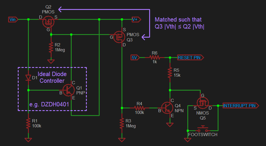
Below is one idea/hack which only uses about an extra 6% of a pin. It adds a couple of components (R1 & the IDC) to R. G. Keen's Advanced Power Switching and Polarity Protection for Effects in order to make the P-MOSFET into an "ideal" diode. Then the gate & source of Q2 are paralleled with those of Q3, such that the two are switched simultaneously: both are on when Vin > V+, both off otherwise. Turning off Q3 also turns off Q4, this does two things: firstly turning on Q5, which has the same effect as holding closed the footswitch with which it shares the input pin; secondly, the reset pin is pulled up to the full 5V from its previous value of a smidge under 4.7V — this is enough such that the microcontroller can differentiate this event from an actual footswitch actuation. Voltages below 4.5V may trigger a reset, 4.7V gives a little wiggle room while still giving about six bits between that value and the 5V maximum (analogue input typically has 10-bit resolution).

From the thread title it should be obvious that particular thread concerns the latter (signal i/o) and relay bypassing (with the logic governed by a microcontroller). Currently there are three major concerns: current draw, circuit/logic complexity, and bypass upon power-loss.
Current Draw
A latching relay clearly wins the first category, requiring only short pulses of current to set the switch to either of the stable positions and otherwise zero current draw.
On the other hand, a non-latching relay requires continuous current through its coil in order to maintain the switch in the non-stable position (most sensibly the position in which effect is active). Most non-latching schemes I've seen use relays specced at around 30mA @ 5V, which in many cases will account for more current than the rest of the circuit combined. However, Panasonic make a line of "high sensitivity" relays which only require around 12mA @ 5V or (if one were to use a higher rated relay running off the main power rail) just 5.6mA @ 9V — this is closer to being acceptable, but we can still go further.
Typically a non-latching relay need only be run at its full rated voltage whilst being actuated; once set this can be reduced: less current is needed to hold the switch in place. According to the Panasonic datasheet the maximum drop-out voltage is below 30%, (after adding some margin) this means it should be possible to have a holding current to around 2mA. I am, however, concerned that doing this presumably must also derate the relay's vibration/shock resistance, but I don't think I've ever seen such a derating specified on any relay's datasheet.
Complexity
The mono-stable nature of a non-latching relay offers simplicity, in that all one has to do in order to reset the relay is stop drawing current through it. As such a non-latching relay ties up the use of at most one GIPO pin — whereas latching relay (whether single or dual coil) would use, by default, two pins — it could be made to use a single pin, but this introduces extra complexity.
A circuit for a non-latching relay can still get relatively complex if wanting to automatically reduce the supplied current to the holding current, especially if you're worrying about minimum set/reset cycle time. If so, you end up with something like this:

When power is applied, and with Q3 turned on, current flows through C1 into the base of Q1 turning it on — thereby giving approximately 9V across (and 5.6mA through) the relay coil K1. As C1 charges the the current through both it and the base of Q1 reduces, eventually turning off the transistor and introducing R1 in series with K1 lowering the current to about 2mA. (When simulated with the shown values and a 2N3904, Q1 begins to turn off at about 20ms.)
Removing power (or turning off Q3) discharges C1. Without Q2, R4 and with D2 replaced with a short, the only path though which C1 could discharge would be via K1, R1 & R3, this current would slow the release of K1: taking around 70ms to decay below the relay's must-release threshold of 560uA. Therefore the current from C1 discharging is instead routed into the base of Q2, turning it on and allowing the cap to discharge much more rapidly via R4 (possibly too fast?). The purpose of diode D2 is to keep Q2 turned on harder for longer, by preventing any (significant) current from bypassing Q2's B-E junction via R3.
Bypass Upon Power-Loss
This is somewhat related to the previous category — a non-latching relay by its very nature gets this for free, to impose this requirement upon a latching relay adds extra circuit complexity. And sure, while it'd be a nice-to-have, I'm not convinced it'd really be that useful.
First one must detect loss of power, then act upon that knowledge whilst the filter caps still hold sufficient charge. Plus, one has to consider if at that specific moment it is okay to attempt to switch the relay: is it in the process of already being switched? Even after the relay is reset, it's not over — any further attempts to re-engage the relay must be blocked also. How complex this gets again is inversely proportional to the number of GPIO pins used: theoretically it would be possible to use the loss of power to trigger a complete bypass the microcontroller and manually reset the relay — however, signalling the μC and doing the logic in code rather than circuitry would be preferable.
Below is one idea/hack which only uses about an extra 6% of a pin. It adds a couple of components (R1 & the IDC) to R. G. Keen's Advanced Power Switching and Polarity Protection for Effects in order to make the P-MOSFET into an "ideal" diode. Then the gate & source of Q2 are paralleled with those of Q3, such that the two are switched simultaneously: both are on when Vin > V+, both off otherwise. Turning off Q3 also turns off Q4, this does two things: firstly turning on Q5, which has the same effect as holding closed the footswitch with which it shares the input pin; secondly, the reset pin is pulled up to the full 5V from its previous value of a smidge under 4.7V — this is enough such that the microcontroller can differentiate this event from an actual footswitch actuation. Voltages below 4.5V may trigger a reset, 4.7V gives a little wiggle room while still giving about six bits between that value and the 5V maximum (analogue input typically has 10-bit resolution).


